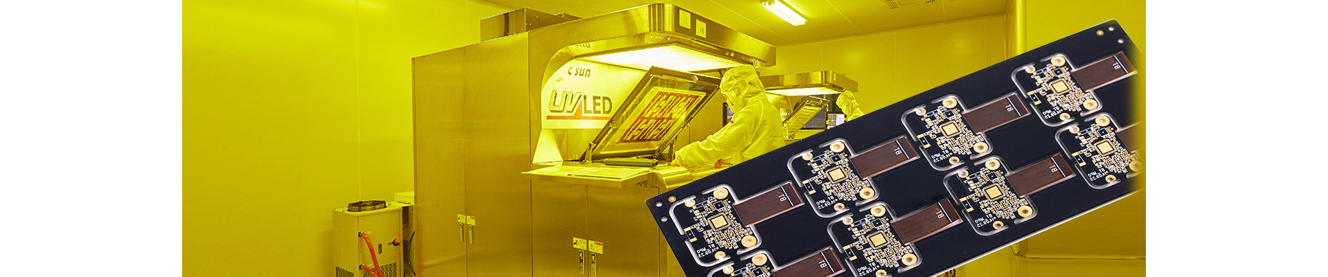
What is Semi-Flex-PCB ? |
|
This technology provides a cost-effective substitute for rigid-flex circuit technology. This is garnered by eliminating the use of more expensive polyimide-based flexible substrates and a streamlined process flow since it requires only one lamination cycle (no lamination cycles if only 2 layers). The flexible portion is achieved by controlled-depth milling away the FR4 material in the bend area. While this allows for multiple bend cycles as shown in limited industry testing, we would recommend this technology only for large radius, flex-to-install bends. |
 |
With simple depth-milling a standard printed circuit board can be prepared for flexible installations. So called "semi-flexible" printed circuits are offering a cost-efficient solution. They save connectors and increase reliability while decreasing size of the application and time needed for assembly. Semi-flexible PCBs are the perfect solution if you have flex-to-install requirements only and there is no dynamic bending during operation. Often layout designers are reluctant to upgrade from a standard PCB with connectors to a notoriously expensive rigid-flexible printed circuit. The advantages are immense, but so are the costs and the layout requirements compared to standard PCBs. Many times this "jump" from standard technology to a high-tech segment is not necessary. Many printed circuits do not require dynamic bending capabilities in operation but only need to be fit into the housing neatly. This is called a "flex-to-install" requirement and here semi-flex offers a really cost-saving alternative technology. |
|
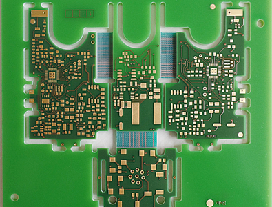
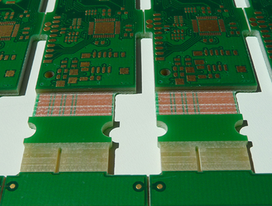
Production of a semi-flexible PCB is identical with the manufacturing process of standard printed circuits. Semi-flexilbe boards can be produced as single-layer, double-layer or multilayer PCBs. With the exemption of a special solder mask that sustains bending, the materials are also identical to standard printed circuits. The only difference happens at the end of the production process when dedicated bending areas are milled down by z-axis routing. The remaining material can be bend and is thin enough to only carry the copper traces and little base material. |
 |
|
|
|
|